p-n Junction Semiconductor Diode | Forward and Reverse Bias | Characteristics
p-n Junction Diode
A p-n junction diode is a p-type semiconductor crystal joined to a n-type semiconductor crystals with using an additional materials for their joining. Symbolically, a semiconductor diode is represented as shown in figure.
 |
| p-n junction Semiconductor Diode |
Here the direction of arrow indicates the direction of conventional current flowing through the diode under the forward biasing arrangement. Thus, p-side of diode may be considered as anode and n-side as the cathode. As the device has two electrodes, it is named as a diode.
No net current flows through a p-n junction diode in an open circuit. However, if we connect some external voltage V across it, the diode is said to be Biased and a current may flow depending upon the nature of biasing. There are two methods of biasing of PN junction diode which are given below :
(i) p-n junction diode under forward bias
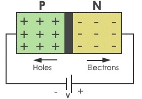
In forward bias arrangement, we apply an external voltage V across a semiconductor diode such that p-side of diode is connected to the positive terminal of the battery and n-side to the negative terminal as shown in figure.
 |
| p-n junction Diode Under Forward bias |
Due to the applied voltage in forward bias, electrons cross the depletion region from n-side to p-side and holes from p-side to n-side. Thus, effectively, electrons and holes are reaching the respective regions where they are minority Carriers. This process is known as 'minority carrier injection'. Due to this concentration gradient, the electrons on p-side diffuse from the junction edge of p-side to other and of p-side. Similarly, holes on n-side diffuse from junction edge of n-side to other end of n-side. This diffusing motions of electrons and holes gives rise to current. The total current in forward bias arrangement of diode is a sum of the hole diffusion current and the conventional current due to electron diffusion.
(ii) p-n junction Diode Under Reverse Bias
In Reverse bias arrangement, we apply an external voltage V across the semiconductor diode such that n-side of diode is connected to positive terminal of voltage supply and p-side to the negative terminal as shown in figure.
 |
| p-n junction Diode Under Reverse bias |
The reverse bias current is almost independent of the applied voltage upto critical reverse Bias Voltage, known as a breakdown voltage. At the reverse current of diode increase sharply and even a slight increase in the Bias Voltage cause last change in current.
V-I Characteristics of semiconductor diode
V-I characteristics of a p-n junction is the curve between voltage across the junction and the circuit current. Usually, voltage is taken along x-axis and the current along y-axis. Figure shows the circuit arrangement for determining the V-I characteristics of a p-n junction diode.
 |
| V-I Characteristics of semiconductor diode |

