Semiconductor Electronics: Materials, Devices and Simple Circuits Class 12 notes Physics Chapter 14
Introduction
In this chapter first, we will discuss the band theory of solids. Then we will discuss junction diode and transistors. After that, we will explore the
basics of Logic gates. In the end, we will take the elementary idea of integrated circuits.
Classification of Metals
On the basis of the relative values of electrical conductivity (σ) or resistivity (ρ = 1/σ ), the solids are broadly classified as:
(i). Metals
They possess very low resistivity (or high conductivity).
ρ ~ 10–2 – 10–8 Ω m
σ ~ 102 – 108 S m-1
(ii). Semiconductors
They have resistivity or conductivity intermediate to metals and insulators.
ρ ~ 10–5 – 106 Ω m
σ ~ 105 – 10-6 S m-1
(iii). Insulators
They have high resistivity (or low conductivity).
ρ ~ 1011 – 1019 Ω m
σ ~ 10-11 – 10-19 S m-1
Classification of Metals on the Basis of Energy Bands
When the atoms come together to form a solid they are so close to each other that the fields of electrons of outer orbits from neighbouring atoms overlap. This makes the nature of electron motion in a solid very different from that in an isolated atom. Inside the solid, each electron has a unique position and no two electrons have the same pattern of surrounding charges.
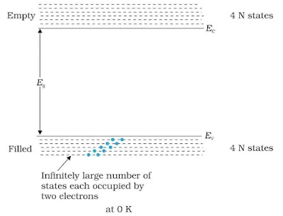
Hence, each electron has a different energy level. These energy levels are so closely packed that we call it an energy band. The energy band which includes the energy levels of the valence electrons is called the valence band. The higher energy band is called the conduction band.
Recommended Books
- NCERT Textbook For Class 12 Physics Part 1 & 2
- CBSE All In One Physics Class 12 2022-23 Edition
- Oswaal CBSE Chapterwise Question Bank Class 12 Physics Book
- Modern's abc Plus of Physics for Class-12 (Part I & II)
Read also: Communication System Class 12 Physics Notes Chapter 15
(i). Metals
In metals, the conduction band and valence band are overlapped to each other. The electrons from the valence band can easily move into the conduction band. Normally, the conduction band is empty but when it overlaps with the valence band, electrons can move freely into it and it conducts electric current through it.
(ii). Semiconductors
In insulators, a large energy band gap exists between the valence band and conduction band. There are no electrons in the conduction band and hence, electrical conduction is not possible under ordinary circumstances. It means that the energy gap is so large that electrons cannot be excited from the valence band to the conduction band by thermal excitation.
Read also: Biomolecules Chemistry Class 12 Notes Chapter 14
(iii). Insulators
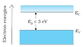
In semiconductors, a small and finite energy band gap exists. Because of the small energy band gap some electrons from the valence band, at room temperature, acquire enough energy to cross the energy gap and enter the conduction band. These electrons are very few and can move in the conduction band. Hence, the resistance of semiconductors is not as high as that of the insulators.
Intrinsic Semiconductor
It is a pure semiconductor without any significant dopant species present. In lattice structures of Ge and Si, each atom is surrounded by four nearest neighbours. Si and Ge have four valence electrons. In its crystalline structure, every Si or Ge atom tends to share one of its four valence electrons with each of its four nearest-neighbuor atoms. These shared electrons form a covalent bond.
In intrinsic semiconductors, the number of free electrons per unit volume (ne) is equal to the number of holes per unit volume (nh).
`n_e=n_h=n_i`
Extrinsic Semiconductor
When a few parts per million (ppm) of a suitable impurity is added to the pure semiconductor, the conductivity increases many times. Such materials are known as extrinsic semiconductors or impurity semiconductors.
In a doped semiconductor, the following relation holds
`n_{e}.n_{h}=n_{i}^2`
Types of Semiconductor
Extrinsic semiconductors are basically of two types:
(i). n-Type Semiconductor
When an impurity atom with 5 valence electrons is doped to a germanium crystal, it replaces one of the germanium atoms. Four of the five valence electrons form covalent bonds with one valence electron of four Ge atoms and the fifth valence electron becomes free to move in the crystal structure. This free electron acts as a charge carrier. Thus by introducing impurity in pure Ge, the number of free electrons increases, and hence the conductivity of the crystal increases. Since the majority of charge carriers in these crystals are negatively charged electrons, they are called n-type semiconductors.
(ii). p-Type Semiconductor
When an impurity atom with 3 valence electrons is doped to a germanium crystal, it replaces one of the germanium atoms. The four germanium atoms surrounding the impurity atom can share one electron each with the impurity atom which has got three valence electrons. for every trivalent impurity atom added, an extra hole will be created. As the trivalent impurity atoms accept electrons from the germanium crystal, it is called acceptor impurity. The Ge crystal so obtained is called a p-type semiconductor as it contains free holes.
p-n Junction
When p- and n-type semiconductors are combined to form a p-n unit, a number of new characteristics appear, which make the combination a very useful device, called the p-n junction diode.
p-n Junction Formation
In the n-region of a p-n junction, the concentration of free electrons is higher than that of holes, whereas in the p-region, the concentration of holes is much higher than that of free electrons. Therefore when a p-n junction is formed, some electrons from the n-region will diffuse into the p-region. Since the hole is nothing but the vacancy of an electron, an electron diffusing from the n- to the p-region simply fills this vacancy, i.e., it completes the covalent bond. This process is called electron-hole recombination.
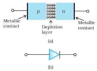
As a result of electron-hole recombination, the electrons in the n-region are neutralized by holes, so in this small region, we are left with only ionized donor atoms. The positive and negative ions in a small region around the junction are bound and are, therefore, immobile. This small region in the vicinity of the junction which has been depleted of free charge carriers and has only immobile ions is called the depletion region.
Semiconductor Diode
A semiconductor diode is basically a p-n junction with metallic contacts provided at the ends for the application of an external voltage. The symbol for the simplest electronic device, namely the p-n junction is shown as. The direction of the thick arrow is from the p to the n-region. The p-side is called the anode and the n-side is known as the cathode.
(i). p-n junction Diode as Forward Bias
If the positive terminal of the battery is connected to the p-side and the negative terminal to the n-side, the junction diode is said to be forward-biased.
(ii). p-n junction Diode as Reverse Bias
If the positive terminal of the battery is connected to the n-side and the negative terminal to the p-side, the junction diode is said to be reverse-biased.
(V-I) Characteristics of Junction Diode
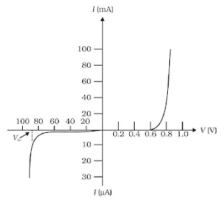
With increasing forward bias the current first increases non-linearly up to a certain forward-biased voltage called knee voltage or cut-in voltage and beyond which the current varies non-linearly.
In the case of reverse bias, the reverse current called reverse saturation current is independent of reverse bias voltage but depends only on the temperature of the junction. If we go on increasing the reverse bias voltage, for a particular value the reverse current increases abruptly. This voltage is called breakdown voltage or Zener voltage.
Avalanche Breakdown
When a reverse bias is applied to the p-n junction, some covalent bonds are broken in the depletion region and electron holes are produced in pairs. These freed electrons move towards the n side under the influence of the barrier electric field, which again collides with atoms producing further electron-hole pairs.
This results in a continuous flow of current carriers in reverse bias and these newly generated charge carriers are also accelerated by the applied electric field in reverse bias leading to avalanche breakdown.
Zener Breakdown
When the reverse bias voltage is increased, the electric field across the depletion region also increases, and if we go on increasing the reverse bias voltage, at a particular value a large number of electrons and holes are produced. This is called Zener breakdown.
Advantages of Semiconductor Diodes
The semiconductor diodes do not produce a humming noise during the operation.
The semiconductor diodes are set into operation as soon as the circuit is switched on.
They are very compact.
Semiconductor diodes require low voltage for their operation. Hence there is low power consumption.
Disadvantage
The main disadvantage of semiconductor diodes is the possibility of their breakdown due to a rise in temperature and the application of high voltage.
Application of Junction Diode as a Rectifier
A rectifier is a device that converts an alternating (AC) input voltage into a direct (DC) output voltage. Any electrical device which has a high resistance to current in one direction and low resistance to current in opposite direction possesses the ability to convert AC current into DC current.
Principle
A p-n junction diode offers very low resistance in forward bias and extremely high resistance in Reverse bias. Due to this property, a p-n junction diode primarily allows the flow of current only in one direction. So, if an alternating voltage is applied across a diode, the current flows only in that part of the cycles when the diode is forward-biased. This property of the p-n junction diode is used to rectify alternating voltages and the circuit used for this purpose is called a rectifier. p-n junction diode can be used either as (a) half-wave rectifier or (b) full-wave rectifier.
(a) Half-wave Rectifier
Construction
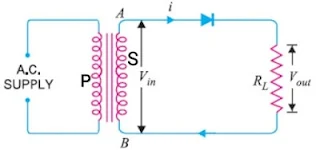
The arrangement for a half-wave rectifier is shown in Fig. The AC input voltage is fed across the primary coil P of a suitable step-down transformer. The secondary coil S of the transformer is connected to the semiconductor p-n junction diode D and a load resistance RL.
Working Method
Let during the first half of the AC input cycle, the end A of secondary S of the transformer be at positive potential and end B at the negative potential. In this situation, the diode is forward biased and a current flows in the circuit. Consequently, an output voltage across load RL is obtained.
During the second half of AC input, the end A of secondary S of transformer is at negative potential and diode D is in reverse bias. So, no current flows through load RL and there is no output voltage across RL.
 |
In the next positive half-cycle of AC input, we again get the output and so on. Thus, we get output voltage as shown in Fig. Here, the output voltage, though still varying in magnitude, is restricted to only one direction and is said to be rectified. Since the rectified output of the circuit is obtained only for half of the input AC wave, the device is called a half-wave rectifier.
(b) Full-wave rectifier
A full-wave rectifier is a rectifier that rectifies both halves of each AC input cycle and gives a unidirectional output voltage continuously.
Construction
In a full-wave rectifier, we use two semiconductor diodes that operate in a complementary mode. The AC input supply is fed across the primary coil P of a center tap transformer. The two ends A and B of the second S of the transformer are connected to the p-ends of the Diodes D1 and D2 respectively. A load resistance RL is connected between the n-terminal of both the Diodes and the center tapping O of the second of the transformer. The DC output is obtained across load residence RL.
Working Method
During the first half cycle of the input voltage, the terminal A is positive with respect to O while B is negative with respect to O. Diode first is forward bias and conducts while diode second is reverse bias and does not conduct, the current flow through RL from D To O. During the second half cycle, A is negative and B is positive with respect to O, thus diode first is reverse bias and diode second is forward biased. The current through RL is in the same direction as during the first half cycle. The resulting output current is a continuous series.
As we are getting output in the positive half as well as the negative half of the AC input cycle, the rectifier is called a full-wave rectifier. Obviously, this is a more efficient circuit for getting rectified voltage or current than a half-wave rectifier.
Special Purpose p-n Junction Diodes
Junction diodes are of many types and find a wide range of applications in electronics. Some of them are discussed below.
(i). Zener diode
The specially designed junction diodes which can operate in the reverse breakdown voltage region continuously without being damaged, are called Zener diodes. These are generally highly doped Silicon diodes. Silicon is preferred over germanium because of its higher thermal stability. A Zener diode is represented by the symbol shown as.
Zener diode as a voltage regulator
An important application of the Zener diode is that it can be used as a voltage regulator. The regulating action takes place because of the fact that in the reverse breakdown region, a very small change in voltage produces a very large change in current. In the Zener region, the resistance of the Zener diode drops considerably.
Let us consider a Zener diode and a dropping resistor R connected to a fluctuating dc supply such that the Zener diode is reverse biased. When the applied voltage is such that the voltage across Zener is less than Zener voltage, the diode will not conduct. Hence, the output voltage will be proportional to the input voltage and is given by `V_{out}=\frac{R_L}{R_S+R_L}V_{In}`, but when the input voltage is such that the voltage developed across the Zener is more than Zener voltage, the diode will conduct and will offer very small resistance.
Hence, it will allow all the extra current, and the output voltage will be equal to Zener voltage i.e., Vout = Vz. But every Zener diode has a certain value of current limit and corresponding power limit. If the current in the Zener diode exceeds this limit, the diode will burn out. Zener diode is always used in reverse bias.
(ii). Photodiode
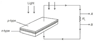
A junction diode made from a photosensitive semiconductor is called a photodiode. In photodiode one region is made so thin that incident light may reach the depletion region.
The photodiode is operated under reverse bias. When the photodiode is illuminated with energy greater than the energy gap (Eg) of the semiconductor, then electron-hole pairs are generated. The construction of a photodiode is such that electron-hole pairs are generated in or near the depletion region of the diode.
Inside the diode, the electric field is such that electrons are collected on N-side, and holes are collected on P-side giving rise to an emf. Hence, when external resistance is connected than current flows through it. The photocurrent is proportional to incident light intensity. Photodiodes can be used as a photodetector to detect optical signals.
(iii). Light-Emitting Diode (LED)
A light-emitting diode is a heavily doped p-n junction encapsulated with a transparent cover so that emitted light can come out. When the forward current of the diode is small the intensity of light emitted is small. As the forward current increases, intensity of light increases and reaches a maximum. Further increase in the forward current results in decrease of light intensity. LEDs are biased such that the light-emitting efficiency is maximum.
LEDs are used in remote controls, burglar alarm systems, optical communication systems, etc. Advantages of LEDs over low-power conventional incandescent lamps are that they have less operational voltages, less power consumption, fast action with no warm-up time, are nearly monochromatic, have long life and ruggedness, and have quick switching on-off capability.
(iv). Solar cell
In a solar cell, one region is made very thin so that most of the light incident on it reaches the depletion region. In this diode when photons of visible light incident to depletion region, electrons jump from the valence band to the conduction band producing electron-hole pairs. These free electrons under the influence of the barrier electric field move to the n region and holes move to the p region, so the potential of the p region increases, and that of n region decreases. A net potential difference develops across the junction.
Junction Transistor
A transistor (also called junction transistor) is a three-terminal semiconductor device in which a p-type or n-type semiconductor is fabricated between two n-type or two p-type layers. There are two types of transistors.
p-n-p transistor.
n-p-n transistor.
(i). p-n-p Transistor
It consists of a very thin layer of n-type semiconductors developed between two thick layers of p-type semiconductors. In this symbolic representation, the direction of the arrow shows the direction of the conventional current. The central part (which is very thin) is called the “base” while the left and right parts are known as the emitter and the collector respectively. The emitter-base (p-n) junction is forward-biased and the base-collector (n-p) junction is reverse-biased in case of active operation of the junction transistor.
Action of p-n-p transistor
The emitter base of p-n-p transistor is forward-biased by connecting it to positive pole of emitter-base battery VEE and the collector is reverse-biased by connecting it to the negative pole of the collector-base battery VCC.
Holes being the majority carriers in emitter are repelled due to forward bias towards the base. As the base is thin and lightly doped, it has a low density of electrons. Therefore, when the holes enter the base region, only about 5% electron-hole combination takes place.
The remaining holes reach the collector under the influence of reverse collector voltage, an electron leaves the negative pole of collector-base battery ECB and neutralizes it. At the same time, an electron from some covalent bond in the emitter enters the positive terminal of EEB, creating a hole in the emitter. Thus, the current in the p-n-p transistor is carried by holes and at the same time, their concentration is maintained as explained above. In this case also,
`I_{e}=I_{b}+I_{c}`
(ii). n-p-n Transistor
It consists of the thin layer of p-type semiconductors developed between two small n-type semiconductors layers.
Action of n-p-n transistor
To understand the action of n-p-n transistor, the n-type emitter is forward - biased by the help of battery VEE and the collector base is reverse-biased by the help of battery VCC.
The electrons being majority carriers in the emitter are repelled due to forward bias towards the base. The base contains holes as the majority of carriers and some holes and electrons combine in the base region but the base is lightly doped. Due to this, the probability of electron-hole combination in the base region is very small (< 5%).
The remaining electrons cross into the collector region and enter the positive terminal of the battery VCC connected to the collector. At the same time, an electron enters the emitter from the negative pole of the emitter-base battery VEE. Thus, in n-p-n transistors, the current is carried inside the transistor as well as in the external circuit by the electrons. If Ie, Ib and Ic are the emitter current, the base current, and the collector current, respectively, then
`I_{e}=I_{b}+I_{c}`
Digital Electronics and Logic Gates
A gate is a logic circuit that has one or more inputs but only one output. It follows a logical relationship between input and output voltages and for this reason, they are called logic gates.
Each logic gate has its characteristic symbol and its function is defined either by a truth table or by a Boolean expression. In digital circuits, low and high voltage is often represented by 0 and 1, respectively.
Truth table: It is a table that shows all input/output possibilities for a logic gate. It is also called a table of combinations.
Boolean expression: George Boole invented a different kind of algebra-based on the binary nature of logic. It was first applied to switching circuits, as a switch is a binary device.
There are three basic logic gates:
(i) OR gate (ii) AND gate, and (iii) NOT gate.
(i). NOT Gate
This is the most basic gate, with one input and one output. It produces an inverted version of the input at its output i.e., it produces a ‘1’ output if the input is ‘0’ and vice versa. This is why it is also known as an inverter.
(ii). OR Gate
In Boolean algebra, the addition symbol (+) is referred to as OR. The Boolean expression Y = A + B implies Y equals A OR B. The OR gate is a device that combines A with B to give Y as the result. The OR gate is two or more inputs and one output device.
(iii). AND Gate
The multiplication sign [dot (.)] is referred to as AND in Boolean algebra. The Boolean expression Y = A . B implies Y equals A AND B. The AND gate is a device that combines A with B to give Y as the result. The AND gate is two or more inputs and one output device.
Combination of Gates
(i). The NAND gate
If the output Y' of AND gate is connected to the input of the NOT gate, the gate so obtained is called the NAND gate. Boolean expression for the NAND gate is `Y = \bar{A.B}`
(ii). The NOR gate
If the output (Y') of the OR gate is connected to the input of a NOT gate, the gate so obtained is called the NOR gate. Boolean expression for the NOR gate is `Y = \bar{A + B}`
Integrated Circuits
In modern days, many logical gates or circuits are integrated in one single ‘chip’. These ‘chips’ are known as integrated circuits (ICs). An IC consists of many passive components like R and C (not L) and active devices like diodes and transistors on a single block (chip) of a semiconductor. The most widely used technology is the monolithic integrated circuit.
Summary
Energy Band: The large number of energy levels confined in a small region of the energy range of a solid are called energy bands. They are of two types, viz., conduction bands and valence bands.
Forbidden Gap: In some solids, there is an energy gap between the conduction band and valence band, called the forbidden gap.
Hole: It is a seat of positive charge which is produced when an electron breaks away from a covalent bond in a semiconductor.
Intrinsic Semiconductor: A pure semiconductor that is free from every impurity is called an intrinsic semiconductor.
Doping: It is a process of deliberate addition of a desirable impurity to a pure semiconductor to modify its properties in a controlled manner.
Extrinsic Semiconductor: A doped semiconductor or a semiconductor with suitable impurity atoms added to it is called an extrinsic semiconductor. They are of two types, viz., N-type (Negative type) and P-type (Positive type).
p-n Junction: When a p-type crystal is brought into close contact with an n-type crystal, the resulting arrangement is called a p-n junction or junction diode.
Diffusion Current means current due to majority carriers and drift current means current due to minority carriers.
Depletion region: It is a layer created around the p-n junction which is devoid of free charge carriers and has immobile ions.
Potential Barrier: Reverse potential difference created in the depletion region.
Forward Biasing: When the positive terminal of the external battery is connected to the p-side and negative to the n-side of the p-n junction, the p-n junction is said to be forward-biased.
Reverse Biasing: A p-n junction is said to be reverse-biased if the positive terminal of the external battery is connected to the n-side and the negative terminal to the p-side of the p-n junction.
AC resistance: It is defined as the ratio of a small change in the voltage (ΔV) applied across the p-n junction to a small change in current ΔI.
Knee Voltage: It is the forward voltage beyond which the current through the junction starts to increase rapidly.
Zener or Breakdown Voltage is the voltage in reverse biasing at which the diode starts conducting. This current is called avalanche current and the region in which this current is established is called the avalanche breakdown region.
The rectifier is a device that converts an alternating current into a direct current. The process is called rectification.
Ripple factor: The ratio of RMS value of AC component to DC component in the rectifier output is called ripple factor.
Junction Transistor: It is a semiconductor device that is obtained by growing a thin layer of one type of semiconductor in between two thick layers of another similar type of semiconductor. It has three terminals (emitter, base, and collector) and two junctions.
Gain of a quantity means its output value upon input value, viz., resistance gain, current gain, voltage gain, power gain etc.
Transconductance or mutual conductance in CE amplifier circuit is defined as the ratio of change in collector current (ΔIc) to the change in input base-emitter voltage ΔVi.
Tank Circuit of a feedback amplifier oscillator is the LC oscillation circuit which provides the signal of desired frequency to the amplifier input.
Analogue Signal: A continuous time-varying current or voltage signal is called an analog signal. An electronic circuit that gives out any type of analog signal is called an analog circuit.
Digital Signal: A signal which has two levels of voltage (represented by 0 or 1) is called a digital signal.
Logic Gates are digital circuits that follow a certain relationship between the input and output voltages.
Truth Table is a table that shows all possible input combinations and the corresponding output for the logic gate.
Boolean Algebra: An English mathematician George Boole developed an ‘Algebra of Logic’ called Boolean Algebra (in his honor) which is based on human reasoning and is ideal for the design and analysis of logic circuits used in semiconductor devices.
In a semiconductor, there are no free electrons at 0 K but the number of free electrons increases with temperature.
The hole behaves as an apparent free particle with an effective positive charge.
Both n-type and p-type semiconductors are electrically neutral. Each logic gate has its characteristic symbol and its function is defined either by a truth table or by a Boolean expression.
In digital circuits, low and high voltage is often represented by 0 and 1, respectively.
Truth table: It is a table that shows all input/output possibilities for a logic gate. It is also called a table of combinations.
Boolean expression: George Boole invented a different kind of algebra based on the binary nature (two-valued) of logic. It was first applied to switching circuits, as a switch is a binary device (on or off).
In an intrinsic semiconductor, the number of free electrons (ne) is equal to the number of holes (nh)
ne = nh = ni
In n-type semiconductor, ne >> nh while in p-type semiconductor nh >> ne.
Zener diode is used for regulating supply voltage so that they are constant.
In the modern-day circuit, many circuits are integrated into one signal ‘chip’. These are known as an integrated circuits (IC).
When the transistor is used in the cut-off or saturation state, it acts as a switch.

